Surface treatment processes enhance the functionality, durability, and aesthetics of materials. This guide provides a detailed overview of key techniques, focusing on their technical aspects, applications, and operational principles. Each method is explained to offer a clear understanding for professionals and manufacturers.
What is Surface Treatment
Surface treatment refers to a range of processes applied to the surface of a material to enhance its properties, such as durability, corrosion resistance, appearance, or functionality. These treatments can include physical, chemical, or mechanical methods like coating, plating, anodizing, painting, or heat treating. For example, metals may undergo galvanizing to prevent rust, while plastics might be treated with UV coatings for improved scratch resistance. Surface treatments are widely used in industries like manufacturing, automotive, and aerospace to extend the lifespan of components, improve aesthetics, or achieve specific performance characteristics tailored to an application.
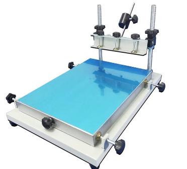
Screen Printing
Screen printing uses a mesh screen, typically made of silk, synthetic fibers, or metal, stretched over a frame. The screen is prepared by creating a stencil where the image areas allow ink to pass through, while non-image areas are blocked. During printing, ink is forced through the open mesh areas onto the substrate using a squeegee. This process is versatile, cost-effective, and suitable for flat or slightly curved surfaces. Common applications include posters, textiles, and product labels.
Key Parameters:
- Mesh count: 100–400 threads per inch, depending on detail and ink type.
- Ink viscosity: 500–5000 cP for optimal flow.
- Squeegee pressure: 20–40 N/cm² for uniform ink transfer.
Applications: Widely used for printing on paper, fabric, glass, and plastics in industries like advertising and apparel.
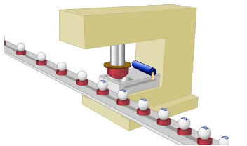
Pad Printing
Pad printing transfers ink from an etched plate to a substrate using a silicone pad. The plate, typically made of steel or plastic, holds the design, and the flexible pad picks up the ink and presses it onto the surface. This method excels in printing on irregular or curved surfaces, such as electronics or medical devices.
Key Parameters:
- Plate depth: 20–30 µm for precise ink transfer.
- Pad hardness: Shore A 20–60, based on substrate shape.
- Ink drying time: 5–20 seconds, depending on formulation.
Applications: Common in electronics for printing on keyboards, phone casings, and instrument panels.
Etching
Etching removes material from a surface using chemical or physical methods to create patterns or textures. Chemical etching involves applying a resist to protect certain areas, then exposing the surface to an etchant like ferric chloride. Dry etching uses plasma or ion beams for precision. This process is critical in electronics and decorative applications.
Key Parameters:
- Etchant concentration: 30–50% for chemical etching.
- Etching time: 5–60 minutes, depending on material and depth.
- Plasma power (dry etching): 100–500 W for controlled material removal.
Applications: Used in circuit board manufacturing, metal decoration, and microfabrication.
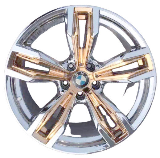
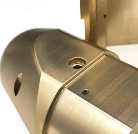
Anodizing
Anodizing is an electrochemical process that forms a protective oxide layer on metals like aluminum. The workpiece acts as the anode in an electrolyte bath, typically sulfuric acid, where oxygen ions bond with the metal surface to create a durable, corrosion-resistant coating. The layer can be dyed for aesthetic purposes.
Key Parameters:
- Electrolyte concentration: 10–20% sulfuric acid.
- Voltage: 12–20 V for standard anodizing.
- Coating thickness: 5–25 µm for decorative or protective purposes.
Applications: Applied in aerospace, automotive, and consumer goods for enhanced durability and appearance.
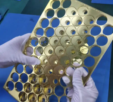
Electroplating
Electroplating deposits a metal layer onto a substrate using an electric current. The substrate serves as the cathode in an electrolyte solution containing metal ions, which are reduced and deposited onto the surface. This enhances corrosion resistance, wear resistance, and aesthetics.
Key Parameters:
- Current density: 1–10 A/dm² for uniform deposition.
- Bath temperature: 20–60°C, depending on the metal.
- Coating thickness: 1–50 µm, based on application.
Applications: Used in jewelry, automotive parts, and electronics for decorative and functional coatings.
PVD (Physical Vapor Deposition)
PVD involves depositing thin films by evaporating or sputtering a material in a vacuum and condensing it onto a substrate. Common methods include thermal evaporation and magnetron sputtering. The resulting films offer high hardness and low friction.
Key Parameters:
- Vacuum pressure: 10⁻³–10⁻⁶ Torr for deposition.
- Deposition rate: 0.1–10 nm/s, depending on material.
- Film thickness: 0.5–5 µm for functional coatings.
Applications: Used in cutting tools, decorative coatings, and optical components.
Water Transfer Printing
Water transfer printing applies decorative patterns to complex surfaces using a water-soluble film with printed designs. The film is placed on water, activated with a chemical, and the substrate is dipped to transfer the pattern. A protective coating is applied afterward.
Key Parameters:
- Water temperature: 25–35°C for optimal film dissolution.
- Activation time: 30–60 seconds for pattern transfer.
- Coating thickness: 10–20 µm for durability.
Applications: Common in automotive interiors, sporting goods, and consumer electronics.
Comparison of Key Surface Treatment Processes
| Process | Substrate Compatibility | Typical Thickness | Primary Application |
|---|---|---|---|
| Screen Printing | Paper, fabric, glass, plastic | 10–50 µm | Posters, textiles, labels |
| Pad Printing | Plastic, metal, glass | 5–20 µm | Electronics, medical devices |
| Etching | Metal, glass, silicon | 1–100 µm | Circuit boards, decorative items |
| Anodizing | Aluminum, titanium | 5–25 µm | Aerospace, automotive |
| Electroplating | Metal, plastic | 1–50 µm | Jewelry, automotive parts |
| PVD | Metal, ceramic, plastic | 0.5–5 µm | Tools, optical coatings |
| Water Transfer Printing | Plastic, metal, wood | 10–20 µm | Automotive, consumer goods |
Considerations for Surface Treatment Selection
Selecting the appropriate surface treatment depends on several factors:
- Material Compatibility: Ensure the process suits the substrate’s properties, such as conductivity for electroplating or heat resistance for PVD.
- Cost Constraints: Processes like screen printing are cost-effective for large runs, while PVD may be expensive due to equipment costs.
- Environmental Impact: Chemical-intensive processes like etching require proper waste management to meet regulations.
- Production Volume: High-volume production benefits from automated processes like electroplating, while low-volume runs may use pad printing.
Conclusion
Surface treatment processes are critical for enhancing material properties and aesthetics across industries. By understanding the technical specifications and applications of methods like screen printing, pad printing, etching, anodizing, electroplating, PVD, and water transfer printing, manufacturers can make informed decisions to meet specific project requirements. The choice of process should balance performance, cost, and environmental considerations.