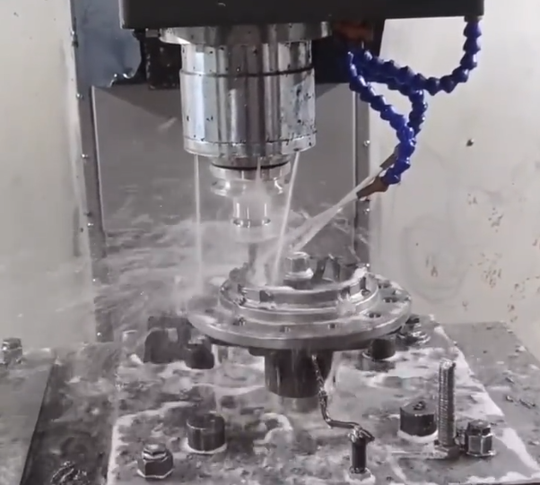
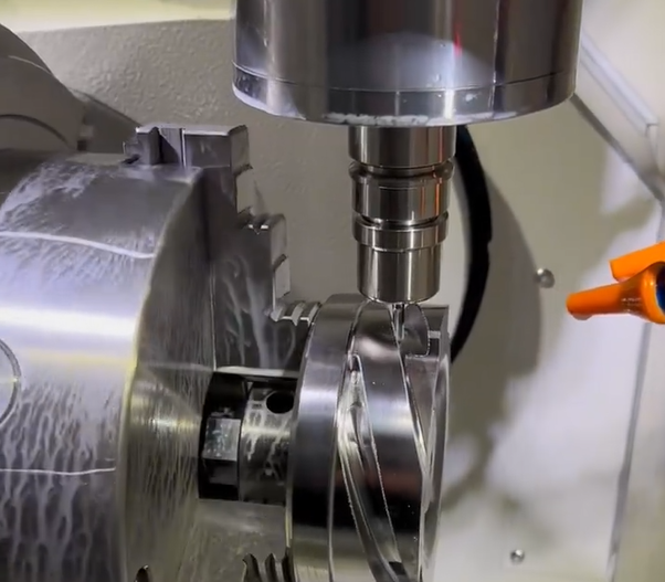
Semiconductor CNC Machining is a specialized manufacturing process that leverages computer numerical control (CNC) technology to produce high-precision components for the semiconductor industry. At Kesu Group, we offer advanced CNC machining services tailored for semiconductor applications, delivering parts with tight tolerances and exceptional quality. Our expertise in CNC milling, CNC turning, and Swiss machining ensures reliable solutions for wafer processing equipment, chip carriers, and other critical semiconductor components.
This article provides a comprehensive overview of semiconductor CNC machining, including its definition, key techniques, material options, surface finishes, benefits, and applications. Whether you’re developing cutting-edge semiconductor devices or need high-volume production, Kesu Group is your trusted partner.
What is Semiconductor CNC Machining?
Semiconductor CNC machining involves the use of CNC technology to fabricate precision components used in semiconductor manufacturing equipment and devices. This process is critical for producing parts with sub-micron tolerances, ensuring the performance and reliability of semiconductor systems. Kesu Group’s semiconductor CNC machining services support both prototyping and high-volume production, catering to the stringent demands of the industry.
Definition and Importance
Semiconductor CNC machining is a subtractive manufacturing process where computer-controlled machinings remove material from a workpiece to create precise components. These components, such as wafer chucks, heat sinks, and connectors, are integral to semiconductor fabrication processes like photolithography, etching, and deposition. The importance of CNC machining in this industry lies in its ability to achieve tolerances as tight as ±0.001 mm, ensuring compatibility with nanoscale semiconductor technologies.
Key Techniques in Semiconductor CNC Machining
Kesu Group employs several CNC machining techniques optimized for semiconductor applications:
- CNC Milling: Utilizes rotating cutting tools to create complex geometries, ideal for producing flat surfaces, slots, and intricate features on semiconductor components.
- CNC Turning: Rotates the workpiece against a stationary tool to fabricate cylindrical parts like wafer carriers and bushings.
- Swiss Machining: Employs sliding headstock lathes for high-precision, small-diameter parts, perfect for connectors and micro-components in semiconductor equipment.
Our advanced multi-axis CNC machinings enable us to handle complex geometries and high-volume production with consistent quality.
Comparison with Other Manufacturing Processes
Unlike additive manufacturing (e.g., 3D printing) or traditional manual machining, CNC machining offers superior precision and repeatability, making it ideal for semiconductor applications. Compared to injection molding, CNC machining is better suited for low-to-medium volume production and rapid prototyping, allowing for quick design iterations without the need for costly molds.
Benefits of Semiconductor CNC Machining
Semiconductor CNC machining provides numerous advantages, making it a preferred choice for manufacturing critical components. Kesu Group’s expertise maximizes these benefits for our clients.
Unmatched Precision
The semiconductor industry demands components with sub-micron accuracy. Kesu Group achieves tolerances as tight as ±0.001 mm for metal parts and ±0.01 mm for plastics, ensuring compatibility with advanced semiconductor processes.
High Volume Capability
Our facilities, equipped with over 100 CNC machinings, support high-volume production of identical parts, from hundreds to millions of units. This scalability ensures cost efficiency and timely delivery for large-scale semiconductor projects.
Material Versatility
Kesu Group works with a wide range of materials, including metals like aluminum, stainless steel, and titanium, and high-performance plastics like PEEK and PTFE, meeting the diverse needs of semiconductor applications.
Rapid Turnaround
Located in China’s Greater Bay Area, Kesu Group benefits from proximity to major shipping ports, enabling fast global delivery. Our streamlined quoting process provides instant feedback, accelerating project timelines.
Kesu Group’s Semiconductor CNC Machining Capabilities
Kesu Group’s state-of-the-art facilities and experienced team make us a leader in semiconductor CNC machining. Our ISO 9001:2015 certification ensures quality and reliability for every component.
Advanced CNC Equipment
Our machining capabilities are supported by a diverse inventory of CNC equipment tailored for semiconductor precision. Below is a table summarizing our key machinings:
| Machine | Quantity | Brand | Max Part Size |
|---|---|---|---|
| 3-Axis CNC Machine | 50 | - | 1500 x 800 mm |
| 4-Axis CNC Machine | 20 | AutoCam | D600 x L1200 mm |
| 3+2 Axis CNC Machine | 10 | AutoCam/TJR | D500 mm |
| 5-Axis CNC Machine | 12 | Jingdiao/DMG/AFMING/Roders | D600 mm |
| 6-Axis CNC Machine | 2 | DMG Mori | D300 x L1200 mm |
| CNC Lathe Machine | 50 | Tsugami | D300 x L1200 mm |
| CNC Swiss Type Automatic Lathe | 23 | Tsugami/Star | D30 x L500 mm |
Inspection Equipment
Quality control is paramount in semiconductor CNC machining. Our inspection equipment ensures every part meets rigorous standards:
| Equipment | Quantity | Brand |
|---|---|---|
| CMM | 3 | LEAD/HEXAGON |
| 2.5D | 3 | - |
| XRF Spectrometer | 1 | HITACHI |
| Altimeter | 3 | - |
| Calliper | 20 | - |
| Micrometer | 10 | - |
Tolerance Standards
Kesu Group delivers exceptional precision for semiconductor components. Below are our best tolerance capabilities:
| Feature | Tolerance of Metal (mm) | Tolerance of Plastic (mm) |
|---|---|---|
| Linear Dimensions | ±0.01 | ±0.05 |
| Diameter | ±0.002 | ±0.02 |
| Precise Hole | ±0.002 | ±0.02 |
| Chamfer Heights | ±0.02 | ±0.05 |
| Angular Dimensions | ±0º5′ | ±1º |
| Straightness | ±0.002 | ±0.02 |
| Flatness | ±0.002 | ±0.01 |
| Perpendicularity | ±0.002 | ±0.01 |
| Symmetry | ±0.002 | ±0.01 |
| Concentricity | ±0.002 | ±0.005 |
| Parallelism | ±0.001 | ±0.01 |
Materials for Semiconductor CNC Machining
Kesu Group supports a wide range of materials optimized for semiconductor applications, ensuring compatibility with cleanroom standards and high-performance requirements.
Metals
Metals are chosen for their strength, conductivity, and thermal properties. Our offerings include:
- Aluminum: Lightweight and corrosion-resistant. Alloys: AL5052-T651, AL6061-T651, AL7075-T651, AL6082-T651.
- Stainless Steel: High strength and corrosion resistance for cleanroom compatibility. Alloys: 201, 303, 304, 316, 410, 420, 17-4PH.
- Titanium: Exceptional strength-to-weight ratio. Alloys: Grade 1, Grade 2, Grade 3, Grade 4, Grade 5.
- Copper: High electrical and thermal conductivity. Alloys: T1, T2, T3, TU1, TU2b.
- Brass: Easy to machine for connectors. Alloys: H59, H62, HA177-2, HMn58-2, HPb59-1, HSn62-1.
Plastics
High-performance plastics are critical for semiconductor components requiring chemical resistance and low outgassing:
- PEEK: High thermal and chemical resistance, ideal for wafer handling. Colors: Opaque beige.
- PTFE (Teflon): Low-friction and chemical-resistant. Colors: Black, White.
- Polycarbonate (PC): Impact-resistant and transparent. Colors: Clear, Black, Glossy.
- Delrin (POM): Low-friction and high-stiffness. Colors: White, Black.
- Nylon: Wear-resistant. Types: PA6, PA66. Colors: White, Black, others.
Material Selection Guide
Selecting the right material depends on factors like thermal conductivity, chemical resistance, and cleanroom compatibility. Below is a table summarizing key materials:
| Material | Properties | Applications |
|---|---|---|
| Aluminum | Lightweight, corrosion-resistant | Heat sinks, wafer chucks |
| Stainless Steel | High strength, cleanroom-compatible | Connectors, fittings |
| PEEK | High thermal and chemical resistance | Wafer handling, insulators |
| PTFE | Low-friction, chemical-resistant | Seals, insulators |
Surface Finishes for Semiconductor CNC Machining
Kesu Group offers a variety of surface finishes to enhance the performance and aesthetics of semiconductor components, ensuring compatibility with cleanroom environments.
Oxidation Finishes
Oxidation finishes improve corrosion resistance and durability:
- Anodizing: Applicable to Aluminum for enhanced corrosion resistance.
- Hard Anodized: Applicable to Aluminum for superior wear resistance.
- Micro Arc Oxidation: Applicable to Aluminum, Magnesium, Titanium.
Electroplating Finishes
Electroplating provides protective and conductive layers:
- Nickel Plating: Applicable to Aluminum, Steel, Stainless Steel, Brass, Bronze, Copper.
- Black & Zinc: Corrosion-resistant finish for Steel, Stainless Steel, Brass, Bronze.
- Zinc Plating: Applicable to Steel, Stainless Steel, Brass, Bronze.
Other Finishes
Additional finishes for semiconductor applications:
- Passivation: Applicable to Steel, Stainless Steel, Brass for enhanced corrosion resistance.
- Polishing: Applicable to Aluminum, Stainless Steel, Brass for a smooth, cleanroom-compatible surface.
- Sandblasting: Applicable to most materials for a matte finish.
- Laser Marking: Applicable to most materials for identification without contamination.
Applications of Semiconductor CNC Machining
Kesu Group’s semiconductor CNC machining services support a range of applications critical to the semiconductor industry:
Wafer Processing Equipment
CNC machining produces precision components like wafer chucks, carriers, and chambers used in photolithography, etching, and deposition processes. Materials like PEEK and stainless steel ensure cleanroom compatibility.
Chip Carriers and Connectors
High-precision connectors and chip carriers are manufactured using Swiss machining and CNC turning, ensuring reliable electrical performance. Copper and brass are commonly used for their conductivity.
Heat Sinks and Thermal Management
Aluminum and copper heat sinks are machined to precise specifications to manage heat in semiconductor devices, ensuring optimal performance and longevity.
Other Applications
Our services extend to components for testing equipment, packaging systems, and cleanroom fixtures, supporting the entire semiconductor manufacturing ecosystem.

Why Choose Kesu Group for Semiconductor CNC Machining?
Kesu Group is a trusted partner for semiconductor CNC machining, offering unmatched precision and scalability. Here’s why clients choose us:
- Advanced Facilities: Over 8,000 square meters with 200+ CNC machinings.
- Expert Team: 200+ employees, including 30+ engineers, ensure flawless execution.
- Global Reach: Serving 3,000+ customers with 500,000+ parts produced annually.
- ISO 9001 Certification: Rigorous quality standards for cleanroom-compatible components.
Frequently Asked Questions (FAQ)
What is Semiconductor CNC Machining?
Semiconductor CNC machining uses CNC technology to produce high-precision components for semiconductor manufacturing equipment and devices, achieving sub-micron tolerances.
What materials are used in semiconductor CNC machining?
Supports metals (aluminum, stainless steel, titanium, copper) and plastics (PEEK, PTFE, polycarbonate) for cleanroom-compatible components.
What tolerances can Kesu achieve?
We achieve tolerances as tight as ±0.005 mm for metal parts and ±0.01 mm for plastic parts, meeting semiconductor industry standards.
What are the applications of semiconductor CNC machining?
It’s used for wafer processing equipment, chip carriers, heat sinks, and cleanroom fixtures in the semiconductor industry.