Precision manufacturing demands rigorous surface defect detection to ensure quality and reliability in micromachined components. This article explores systematic approaches, equipment, and parameters for identifying defects in micromachining processes.
Overview of Surface Defects in Micromachining
Micromachining produces components with feature sizes ranging from 1 to 500 micrometers, often used in industries like aerospace, medical devices, and electronics. Surface defects such as scratches, pits, cracks, and burrs can compromise functionality and reliability. These defects arise from tool wear, material inconsistencies, or process parameter deviations. Effective detection requires high-resolution imaging and precise measurement techniques tailored to microscopic scales.
Defect detection must account for surface texture, characterized by roughness parameters like Ra (arithmetic average roughness) and Rz (maximum height of the profile). For instance, a typical Ra value for micromachined surfaces is 0.02–0.2 µm, and defects smaller than 1 µm must be identified to meet stringent standards.
Key Methods for Surface Defect Detection
Several methods are employed to detect surface defects in micromachining, each with specific advantages and limitations. The choice depends on defect size, material properties, and production requirements.
Machine Vision-Based Inspection
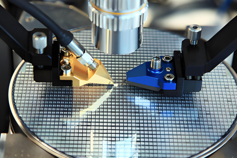
Machine vision systems use high-resolution cameras and image processing algorithms to identify defects. These systems are non-contact, fast, and suitable for automated production lines. A typical setup includes a CMOS camera with a resolution of 5–20 megapixels, paired with a telecentric lens offering a magnification of 10x–100x. Illumination is critical, with coaxial or ring lighting at 5000–6500 K color temperature ensuring uniform exposure.
Image processing involves edge detection (e.g., Canny algorithm), thresholding, and pattern matching. For example, a scratch with a width of 2 µm can be detected using a pixel resolution of 0.5 µm/pixel. Calibration ensures accuracy, with reference standards like NIST-traceable grids used to verify measurements.
Laser Scanning and Profilometry
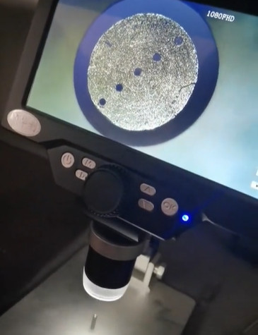
Laser scanning measures surface topography by projecting a laser beam and analyzing reflected light. Confocal laser scanning microscopes achieve vertical resolutions of 1–10 nm and lateral resolutions of 0.1–0.5 µm. These systems are ideal for detecting pits and cracks with depths as small as 0.05 µm.
Key parameters include laser wavelength (typically 405–635 nm) and scanning speed (0.1–10 mm/s). Data processing involves 3D reconstruction and filtering to remove noise. For instance, a Gaussian filter with a cutoff wavelength of 0.8 µm is often applied to isolate defects from surface roughness.
Scanning Electron Microscopy (SEM)
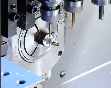
SEM provides high-magnification imaging (up to 100,000x) and is used for detailed defect analysis. It operates by scanning a sample with an electron beam, achieving resolutions of 1–5 nm. SEM is particularly effective for conductive materials like metals but requires vacuum conditions, limiting its use in production lines.
Sample preparation involves cleaning and coating non-conductive surfaces with a 5–10 nm gold layer. Imaging parameters include accelerating voltage (5–20 kV) and probe current (10–100 pA). SEM is often used for failure analysis rather than routine inspection due to its complexity.
Acoustic Microscopy
Acoustic microscopy uses ultrasonic waves to detect subsurface defects like voids or delaminations. It operates at frequencies of 50–200 MHz, with a spatial resolution of 5–20 µm. This method is non-destructive and suitable for composite materials used in micromachining.
A typical setup involves a piezoelectric transducer and a coupling medium (e.g., deionized water). Signal analysis identifies anomalies based on amplitude and time-of-flight variations. For example, a void with a diameter of 10 µm can be detected at a depth of 50 µm.
Equipment and System Specifications
Selecting appropriate equipment is critical for reliable defect detection. The following table summarizes common systems and their specifications:
| Method | Equipment | Resolution | Inspection Speed | Material Suitability |
|---|---|---|---|---|
| Machine Vision | CMOS Camera, Telecentric Lens | 0.5–2 µm | 10–100 parts/min | Metals, Polymers |
| Laser Scanning | Confocal Microscope | 1–10 nm (vertical) | 0.1–10 mm/s | Metals, Ceramics |
| SEM | Electron Microscope | 1–5 nm | 1–5 samples/hour | Conductive Materials |
| Acoustic Microscopy | Ultrasonic Transducer | 5–20 µm | 1–10 cm²/min | Composites, Polymers |
Practical Considerations in Defect Detection
Implementing defect detection systems involves several practical considerations to ensure accuracy and efficiency.
Environmental Control
Vibration, temperature, and humidity affect measurement accuracy. For instance, a temperature variation of ±1°C can cause thermal expansion of 0.01–0.1 µm in steel components. Vibration isolation tables with damping frequencies below 10 Hz are recommended. Cleanroom conditions (ISO Class 5–7) minimize particle contamination, which can be mistaken for defects.
Calibration and Maintenance
Regular calibration using certified standards ensures measurement traceability. For machine vision systems, a calibration grid with 10 µm pitch is used monthly. Laser scanners require annual recalibration of optics and stages. Maintenance includes cleaning lenses and replacing worn components like laser diodes after 10,000 hours of operation.
Data Management
Defect detection generates large datasets, especially with 3D imaging. A single laser scan of a 1 mm² area at 0.1 µm resolution produces 100 MB of data. Efficient storage (e.g., SSDs with 10 TB capacity) and processing (e.g., GPUs with 16 GB VRAM) are essential. Software like MATLAB or Python with OpenCV libraries is used for analysis.
Limitations and Constraints
While advanced methods enhance detection capabilities, certain limitations persist. Machine vision struggles with transparent or highly reflective surfaces, requiring specialized lighting. Laser scanning is time-consuming for large areas, with a 1 cm² scan taking 5–10 minutes. SEM’s vacuum requirement and sample preparation limit throughput. Acoustic microscopy has lower resolution compared to optical methods, making it less suitable for surface defects smaller than 5 µm.
Material properties also pose challenges. For example, ceramics with high hardness may resist scratching but are prone to micro-cracks, which are harder to detect. Polymers, due to their flexibility, may exhibit transient defects that disappear under stress relaxation.
Conclusion
Detecting surface defects in micromachining requires a combination of advanced methods, precise equipment, and rigorous process control. Machine vision offers speed and automation, laser scanning provides high resolution, SEM delivers detailed imaging, and acoustic microscopy excels in subsurface inspection. By selecting appropriate techniques and addressing practical considerations, manufacturers can achieve consistent quality in micromachined components. Systematic implementation ensures reliability, meeting the demands of precision industries.